Combinational Logic Circuits Lab Report
View Lab Report Combinational Logic Circuit docx from BENG 2211 at Technical University of Malaysia Melaka. Protoboard 1 7400 1 7402 1 7404 1 74175.
L04 Combinational Logic
The half adder The half adder is the simpler of the two types of adders as it does not use a carry input from a previous stage.
. View Lab Report - Lab 8 Combinational Logic Circuit IIdocx from ENG 100 at University of California Davis. Lab 8 Combinational Logic Circuit II Objective and Introduction. Digital Logic Circuit Analysis and Design 1995 Victor P.
Be sure to read the laboratory assignment carefully and answer all questions in your lab report. Materials that you need For this lab you will need the following parts. Familiarize students with laboratory equipment operation of fundamental logic gates and design and construction of combinational logic circuits based.
State any pertinent thoughts or conclusions that you made in course of performing the lab. Readings provide insight into finding minimal realizations of combinational logic not only in terms of logic gates but also chip count. Connect Input A on switch S7 Input B on switch S6 Input C on switch S5 andconnect output X on LED 7.
This EE 2310 lab exercise reinforces the classroom lectures on combinational logic. Combinational logic circuit lab report Recovered on 29 July 2003 Only the combinations that produce a production of 1 are maintained because the Boolean equation intends to represent a quantitative function for when the result will have a Value of the truth when a fee is charged in the example of the ATM machine. In addition you will go over mixed logic.
Lab Report ELE 2213 ELE 2213 Digital Circuits CLO-2 Analyze combinational logic circuits using logic symbols truth tables and Boolean equations. Lab grade will depend on the working of the circuit and will be checked off by the lab instructor. Cascading smaller combinational circuits into larger circuits as well as the basics of a bus structure will be investigated.
Include the Boolean algebra truth tables and logic diagrams for each. Carroll H Troy Nagle David Irwin ISBN-13. This modified circuit works the same as the given alarm circuit and shows the exact truth table result.
Combinational Circuits 1 Objective In this experiment you will learn about designing combinational circuits with discrete parts such as the NAND NOR and voltage inverter. In lab a combinational circuit will be investigated. SEMESTER 1 20202021 FACULTY OF ELECTRONICS AND COMPUTER ENGINEERING BENG.
This lab will be having Study Resources. One example of the combinational circuit is the binary adder. Abdelkader Tami Student Name Student ID Number Abraham Ande H00396342 Abdulla Eisa Ibrahim Albahlooli H00348836.
Lab 2 Ð 1 Ð Combinational Logic Cir cuits Object T o investig ate the properties of combinational logic circuits as illustrated by the half adder full adder and data selec-tormultiple xer. Many of the labs will contain questions. Lab 1 Basic Logic Circuits Instructor.
The 74LS Low-power Schottky family like the original uses TTL StudentShare Our website is a unique platform where students can share their papers in a matter of giving an example of the work to be done. They provide experience with common 7400 digital circuits. Digital Logic Lab Lab Report Experiment 2 c Use the breadboard in Figure 2 and mark using a color pen or pencil or importto Paint all the necessary connections to build the circuit shown in Figure 1.
Lab 4 - Combinational Logic Circuits Clevin Cevallos Experimental procedure Use Multisim to construct the original expressions then simplify the expression and construct the new logic circuit. P a rts 1 7400 Quad 2 input N AND g ate 1 7408 Quad 2 input AND g ate 2 7486 Quad 2 input XOR g ate. Compare the truth tables of both to check that they are the same.
Goal of this exercise. QUESTIONS AND ANSWERS REQUIRED IF APPLICABLE. The report Introduction to the Combinational Logic Circuit calculates modification which can be obtained by using AND gate in place of NAND gate and by removing inverter Z from the output end.
The paper Combinational Logics tells us about several families of logic ICs. You should provide sufficient and substantial answers. Ad Browse Discover Thousands of Reference Book Titles for Less.
Combinational circuits do not retain information as do sequential circuits and their outputs change with any change in input.

Pdf Combinational Logic Gates And Circuits Mahroo Uris Academia Edu

Combinational Logic Circuits Using Logic Gates
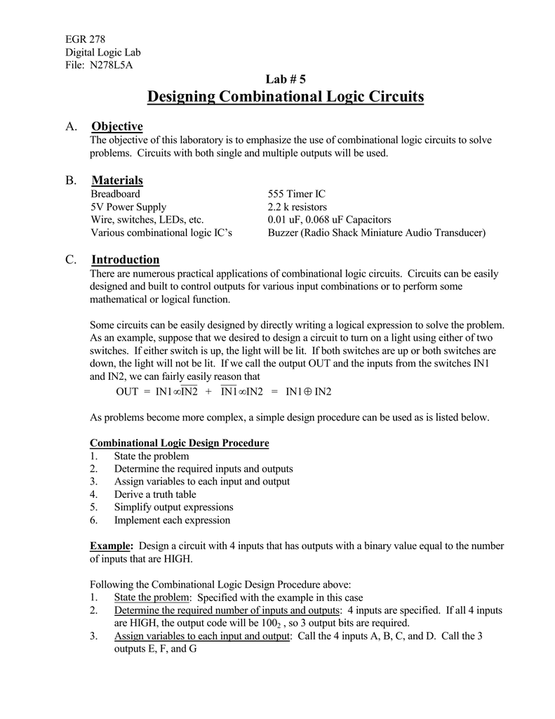
Designing Combinational Logic Circuits
L04 Combinational Logic

Combinational Circuit Analysis Example Given This Logic Circuit

Experiment Write Vhdl Code For Realize All Logic Gates Logic Coding Computer Science Programming


Comments
Post a Comment